Unlock IMPORTANT QUESTION
This question was bookmarked by 5 NEET 2025 toppers during their NEETprep journey. Get Target Batch to see this question.
✨ Perfect for quick revision & accuracy boost
Buy Target Batch
Access all premium questions instantly

If ne and vd be the number of electrons and drift velocity in a semiconductor. When the temperature is increased

(1) ne increases and vd decreases

(2) ne decreases and vd increases

(3) Both ne and vd increases

(4) Both ne and vd decreases

Subtopic:  Types of Semiconductors |
 51%
Level 3: 35%-60%
Hints

Unlock IMPORTANT QUESTION
This question was bookmarked by 5 NEET 2025 toppers during their NEETprep journey. Get Target Batch to see this question.
✨ Perfect for quick revision & accuracy boost
Buy Target Batch
Access all premium questions instantly

The energy gap of silicon is 1.14 eV. The maximum wavelength at which silicon will begin absorbing energy is

(1) 10888 Å                   

(2) 1088.8 Å

(3) 108.88 Å                   

(4) 10.888 Å

Subtopic:  Energy Band theory |
 63%
Level 2: 60%+
Hints

Unlock IMPORTANT QUESTION
This question was bookmarked by 5 NEET 2025 toppers during their NEETprep journey. Get Target Batch to see this question.
✨ Perfect for quick revision & accuracy boost
Buy Target Batch
Access all premium questions instantly

Which of the following energy band diagram shows the N-type semiconductor


1. 

2. 

3. 

4. 

Subtopic:  Energy Band theory |
 81%
Level 1: 80%+
Hints

Unlock IMPORTANT QUESTION
This question was bookmarked by 5 NEET 2025 toppers during their NEETprep journey. Get Target Batch to see this question.
✨ Perfect for quick revision & accuracy boost
Buy Target Batch
Access all premium questions instantly

Which of the energy band diagrams shown in the figure corresponds to that of a semiconductor


1. 
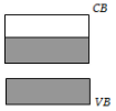
2. 

3. 

4. 

Subtopic:  Energy Band theory |
 54%
Level 3: 35%-60%
Hints

Unlock IMPORTANT QUESTION
This question was bookmarked by 5 NEET 2025 toppers during their NEETprep journey. Get Target Batch to see this question.
✨ Perfect for quick revision & accuracy boost
Buy Target Batch
Access all premium questions instantly

The energy band diagrams for three semiconductor samples of silicon are as shown. We can then assert that

(1) Sample X is undoped while samples Y and Z have been doped with a third group and a fifth group impurity respectively

(2) Sample X is undoped while both samples Y and Z have been doped with a fifth group impurity

(3) Sample X has been doped with equal amounts of third and fifth group impurities while samples Y and Z are undoped

(4) Sample X is undoped while samples Y and Z have been doped with a fifth group and a third group impurity respectively

Subtopic:  Energy Band theory |
 75%
Level 2: 60%+
Hints

Unlock IMPORTANT QUESTION
This question was bookmarked by 5 NEET 2025 toppers during their NEETprep journey. Get Target Batch to see this question.
✨ Perfect for quick revision & accuracy boost
Buy Target Batch
Access all premium questions instantly

In a semiconducting material, the mobilities of electrons and holes are \(\mu_e\) and \(\mu_{h}\) respectively. Which of the following is true?
1. \(\mu_{e} > \mu _{h}\)
2. \(\mu_{e} < \mu _{h}\)
3. \(\mu_{e} = \mu _{h}\)
4. \(\mu_{e} <0; ~\mu _{h}>0\)

Subtopic:  Types of Semiconductors |
 69%
Level 2: 60%+
Hints

Unlock IMPORTANT QUESTION
This question was bookmarked by 5 NEET 2025 toppers during their NEETprep journey. Get Target Batch to see this question.
✨ Perfect for quick revision & accuracy boost
Buy Target Batch
Access all premium questions instantly

The temperature (T) dependence of resistivity (ρ) of a semiconductor is represented by

1. 

2. 

3. 

4. 

Subtopic:  Energy Band theory |
 73%
Level 2: 60%+
Hints

Unlock IMPORTANT QUESTION
This question was bookmarked by 5 NEET 2025 toppers during their NEETprep journey. Get Target Batch to see this question.
✨ Perfect for quick revision & accuracy boost
Buy Target Batch
Access all premium questions instantly

In a forward biased P-N junction diode, the potential barrier in the depletion region is of the form

1. 

2. 

3. 

4. 

Subtopic:  PN junction |
 56%
Level 3: 35%-60%
Hints

Unlock IMPORTANT QUESTION
This question was bookmarked by 5 NEET 2025 toppers during their NEETprep journey. Get Target Batch to see this question.
✨ Perfect for quick revision & accuracy boost
Buy Target Batch
Access all premium questions instantly

Different voltages are applied across a P-N junction and the currents are measured for each value. Which of the following graphs is obtained between voltage and current?

1. 

2. 

3. 

4. 

Subtopic:  PN junction |
Level 3: 35%-60%
Hints

Unlock IMPORTANT QUESTION
This question was bookmarked by 5 NEET 2025 toppers during their NEETprep journey. Get Target Batch to see this question.
✨ Perfect for quick revision & accuracy boost
Buy Target Batch
Access all premium questions instantly

If the following input signal is sent through a PN-junction diode, then the output signal across RL will be


1. 

2. 

3. 

4. 

Subtopic:  PN junction |
 82%
Level 1: 80%+
Hints