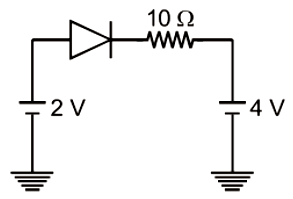
The current through an ideal p-n junction diode shown in the circuit will be:

1. 5 A
2. 0.2 A
3. 0.6 A
4. zero

2. 0.2 A
3. 0.6 A
4. zero


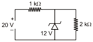
1. 36 mW
2. 12 mW
3. 144 mW
4. 64 mW
A semiconductor is known to have an electron concentration of \(8\times 10^{13}~\text{cm}^{-3},\) and a hole concentration of \(5\times 10^{2}~\text{cm}^{-3}.\) The semiconductor is:
| 1. | \(\mathrm{n}\text-\)type | 2. | \(\mathrm{p}\text-\)type |
| 3. | intrinsic | 4. | insulator |
In the given figure, the potential difference between \(A\) and \(B\) is:
| 1. | \(0\) | 2. | \(5\) volt |
| 3. | \(10\) volt | 4. | \(15\) volt |
The conductivity of an n-type semiconductor whose density of conduction electrons is , Density of holes is , Mobility of conduction electrons is and Mobility of holes is will be
1.
2.
3.
4.
1. \(n_i=n_e=n_h\)
2. \(n_i^2=n_en_h\)
3. \(n_h>> n_e\)
4. \(n_h<<n_e\)
Which of the following is correct for \(\mathrm{n}\)-type semiconductors?
| 1. | electron is the majority carriers and trivalent atoms are dopants. |
| 2. | electrons are majority carriers and pentavalent atoms are dopants. |
| 3. | holes are majority carriers and pentavalent atoms are dopants. |
| 4. | holes are majority carriers and trivalent atoms are dopants. |
When a transistor is used as a switch it is in:
1. Active state
2. Cut off state
3. Saturation state
4. Both cut off state and saturation state are possible
| 1. | the depletion region becomes thick. |
| 2. | the \(\mathrm{p}\text-\)side is at a higher potential than \(\mathrm{n\text-}\)side. |
| 3. | the current flowing is zero. |
| 4. | the effective resistance is of the order of \(10^6 ~\Omega\). |

